Solving the trouble caused by thermal deformation of RF components: Ways to reduce interface thermal resistance
The logic of thermal stress deformation of RF components can be summarized as a clear causal chain:
Material CTE mismatch (root cause) → Temperature fluctuations (heating/environmental temperature changes, directly triggered) → Structural constraints (fixed/encapsulated, limiting expansion) → Stress accumulation cannot be released → Component warping, cracking, and other deformations.
Therefore, the core idea for solving thermal stress deformation also revolves around three directions: "reducing CTE differences (selecting matching materials)", "controlling temperature fluctuations (strengthening heat dissipation)", and "releasing constraints (elastic fixation)" (such as the phase change thermal paste you previously focused on, which is one of the solutions for buffering constraints through "elasticity+fluidity").
Direct cause: temperature fluctuations (heating+environmental temperature changes)
1. Component itself generates heat during operation (main heat source)
RF components (such as power amplifiers, RF switches, and filters) generate Joule heat due to current passing through the components during operation, leading to a rapid increase in local temperature (some high-power modules can rise from room temperature to 80-120 ℃): the heat is concentrated in the core area of the chip, forming a temperature gradient between the "local high temperature zone" (such as the chip surface) and the "low temperature zone" (such as the edge of the casing); Due to temperature differences, different regions of the same material experience varying degrees of expansion (with more expansion in high-temperature areas and less expansion in low-temperature areas), resulting in internal "thermal stress" and causing local deformation (such as upward warping of chip edges).
2. External environmental temperature cycle
RF equipment often needs to adapt to complex environments (such as outdoor base stations, vehicle mounted RF modules), facing temperature cycles caused by day night temperature differences, seasonal changes, or equipment on/off (such as -40 ℃~60 ℃): the components shrink as a whole at low temperatures, and expand as a whole at high temperatures. Repeated "shrinkage expansion" can cause periodic changes in stress;
Structural constraints (fixed/encapsulated limitations)
1. Rigid fixation around (most typical scenario)
Fixed around the RF component (such as attached to the heat dissipation base/housing through screw locking): When the component is heated, it should expand freely in all directions, but the rigid fixation of the screws limits the direction of expansion; The expansion force is "blocked" by the screw and converted into internal stress, causing the center of the component to protrude upwards (warp deformation) - this is also the direct cause of the "poor contact of thermal interface materials and increased thermal resistance" you encountered before.
2. The rigidity of the packaging structure is too highSome RF components adopt fully sealed metal packaging (JUN level RF modules), and the stiffness of the packaging shell is much greater than that of the internal substrate and chip: the shell will hardly deform due to temperature changes, while the internal substrate and chip will expand normally; The shell forms a "rigid cage" that transfers all the stress generated by internal expansion to the chip and substrate, which can easily lead to substrate cracking or detachment of solder joints between the chip and substrate (such as BGA solder joint cracking).
3. Constraints on interface connections (thermal conductive materials, adhesives)
The connection layers inside the component (such as solder between the chip and the substrate, thermal interface materials) can also become constraint points: if the thermal material is rigid (such as ceramic tiles), or if the adhesive has high hardness after curing, it will limit the relative expansion between the chip and the substrate; When the temperature changes, the connecting layer will convert the expansion difference between the two into shear stress, causing the connecting layer to peel off or crack, while driving the overall deformation of the component.
Select measures
Based on the cost-effectiveness ratio, it is recommended to prioritize the following measures: first choice: optimizing thermal conductivity materials (low-cost, easy to implement) - using phase change thermal paste for medium to low deformation, elastic thermal pads for medium to high deformation, and liquid metal for high heat flux density; Second choice: Structural and material optimization (with good long-term effect) - replace with a low CTE substrate and use elastic fixation method to reduce deformation from the root; Assist: Process control (details determine success or failure) - control torque, interface cleaning, aging pretreatment to ensure initial fit.
Car mounted RF amplifier module: Low CTE AlN substrate+floating screws around (with silicone washers)+chip mounted heat dissipation plate+elastic thermal pad (thermal conductivity coefficient 8 W/(m · K)) between the heat dissipation plate and the housing, which can reduce thermal deformation by 60% and interface thermal resistance by more than 40%.

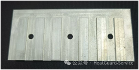
Figure 1 Graphite aluminum based isothermal plate
Fill the gaps with "deformation compensation type thermal conductive material" and repair the contact
The direct consequence of thermal deformation is the appearance of micro/macro gaps at the interface. Therefore, choosing a thermal interface material (TIM) that can actively "adapt to deformation and fill gaps" is the most direct way to reduce thermal resistance. The compensation ability and applicable scenarios of different materials vary greatly,
Phase change thermal conductive paste


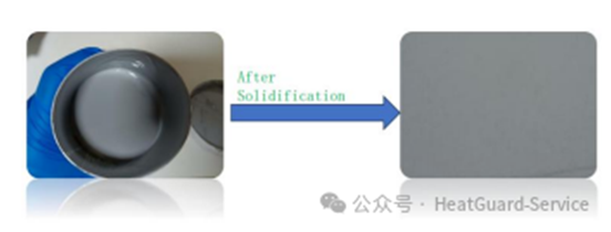
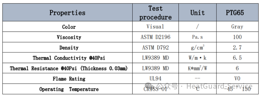
At room temperature, it is solid and melts into a paste after thermal deformation (reaching the phase transition temperature of 45 ℃), automatically filling gaps; After phase transition, the viscosity is low and it can penetrate into micro cracks (10-50 μ m), maximizing the contact area; After curing, it has a certain degree of elasticity and can cushion subsequent slight deformations. Low to medium deformation scenarios (such as component warpage<0.5mm), such as RF power modules and small filters.
Liquid metal thermal conductive agent


At room temperature, it is liquid (such as gallium indium alloy), with extremely strong fluidity, and can completely fill any shape of gap; Extremely high thermal conductivity (50-100 W/(m · K)), close to that of metals; Non volatile, non aging, corrosion-resistant, and has good long-term stability. Large deformation+high heat flux density scenario (such as high-power RF amplifier, heat flux density>50 W/cm ²).

