Diamond substrate technology: a key technology empowering the next generation of semiconductors
With the rapid development of technology and the increasing global demand for high-performance and high-efficiency semiconductor devices, the importance of semiconductor substrate materials as a key technological link in the semiconductor industry chain is becoming increasingly prominent. Semiconductor substrate materials are the foundation for manufacturing semiconductor devices and integrated circuits, and their performance directly affects the quality and performance of the final product. Traditional substrate materials are no longer able to meet the demands of these emerging fields. Therefore, finding and developing new generation high-performance semiconductor substrate materials has become an inevitable trend in the industry's development.
01
Single crystal diamond has an ultra wide bandgap, low dielectric constant, high breakdown voltage, high intrinsic electron and hole mobility, and superior radiation resistance, making it the best known wide bandgap high-temperature semiconductor material. Compared to conventional semiconductor material silicon, diamond's excellent thermal conductivity can timely dissipate heat during circuit operation, greatly improving the operating power of precision instruments and avoiding damage to various electronic devices caused by heat accumulation. In addition, the saturated carrier velocity of diamond is superior to other semiconductor materials, coupled with high electron mobility and extremely high breakdown electric field, making it an ideal substrate material for high-frequency semiconductor devices. With the arrival of the 5G communication era, the application of diamond in high-frequency power devices and other fields is becoming increasingly important. Japan and other countries have successfully developed mass production methods for ultra-high purity large-sized diamond wafers, demonstrating their strong application potential.
Common semiconductor material parameters

02
In the manufacturing process of semiconductor devices, the production technology of substrate materials is one of the key links that determine device performance. This process includes crystal growth, substrate preparation and processing, as well as subsequent surface treatment techniques, each step of which has a profound impact on the quality and performance of the final product.
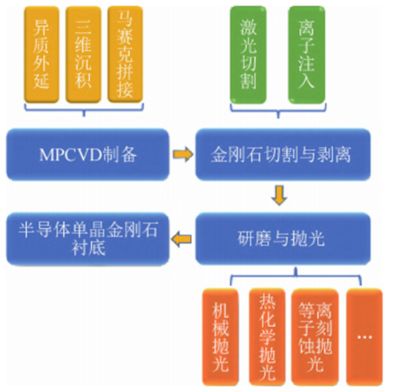
Preparation process of semiconductor single crystal diamond substrate
(1) Preparation of Single Crystal Diamond
The synthetic diamond industry mainly has two preparation methods: high temperature and high pressure method (HTHP) and chemical vapor deposition method (CVD). Among them, CVD method has become the mainstream method for preparing diamond semiconductor substrates due to its advantages of high pressure resistance, high radio frequency, low cost, and high temperature resistance. In theory, as long as a substrate of sufficient size can be obtained, single crystal diamond of the corresponding size can be prepared. According to different substrate types, CVD deposition of diamond can be divided into heteroepitaxy and homoepitaxy. Due to the difficulty in obtaining high-quality single crystal diamond substrates, choosing a suitable heterogeneous substrate for epitaxial growth of single crystal diamond is undoubtedly the optimal choice for preparing inch sized single crystal diamond.
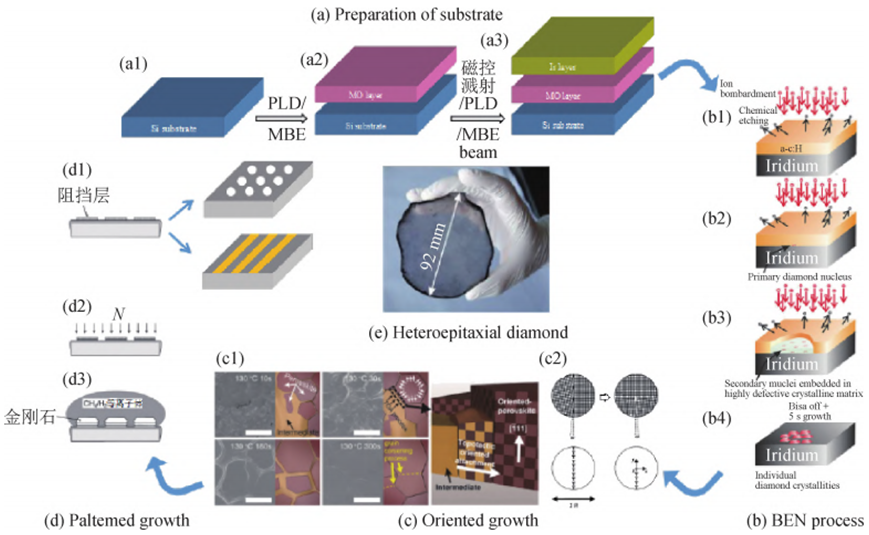
Schematic diagram of heterogeneous epitaxial deposition of large-sized single crystal diamond
(2)Cutting and peeling
Large sized single crystal diamond needs to be cut into a certain shape and thickness. The excessive losses generated by conventional wire cutting and mechanical processing limit the utilization rate of large-sized single crystal diamond and are not suitable for cutting large-sized single crystal diamond. The principle of laser cutting is that under the irradiation of laser, the diamond material vaporizes instantly. Due to the short action time and small spot of laser, it has a series of advantages such as fast speed and narrow cutting gap, and is often used for cutting large-sized single crystal diamond.
To remove the CVD diamond layer from the seed crystal, ion implantation technology is required. When using laser cutting to separate epitaxial layers, a portion of the diamond will be lost, and the proportion of loss increases with the size of the diamond wafer. Ion implantation technology uses high-energy particles to bombard the substrate in advance, forming a non diamond phase about a few hundred nanometers below the surface of the pre polished diamond seed crystal. The depth of the damage layer is determined by the energy of the injected ions. After ion implantation, the diamond seed crystal continues to grow single crystal diamond using homoepitaxial technology, and then the non diamond phase is removed using electrochemical corrosion technology to achieve the purpose of separating the substrate.
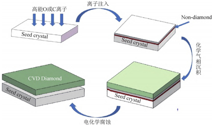
Roadmap for Stripping Technology of Large Single Crystal Diamond
(3)Polishing
Polishing technology plays an important role in the preparation of high-quality single crystal diamond substrates, which mainly includes two aspects: firstly, polishing can be used to prepare seed crystals for CVD homoepitaxial growth of single crystal diamond, and the surface quality of the seed crystals will directly affect the growth quality of single crystal diamond; Secondly, polishing can be used to prepare high-quality single crystal diamond substrates. At present, after growing CVD single crystal diamond, many defects usually appear on its surface, so it is necessary to flatten and polish it.
Mechanical polishing (MP): MP is a polishing process that uses diamond and high-speed rotating polishing discs (cast iron discs, sanding discs) to generate brittle fracture and remove surface materials through friction. At the same time, due to the high temperature generated by the friction between the high-speed rotating polishing disc and diamond, the high temperature provides the driving force for the transition from "hard" diamond to "soft" graphite. By combining micro cutting and graphitization principles, diamond polishing is achieved.
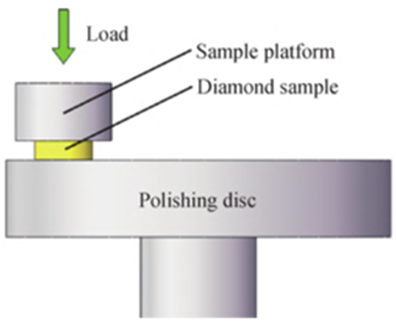
Schematic diagram of MP principle
Advantages: The device has the characteristics of simple principle, easy operation, high efficiency, and suitability for large-scale production. It can achieve a relatively smooth and flat surface, and is suitable for rough, medium, and fine polishing.
Disadvantages: The high temperature generated during high-speed friction can damage the polishing disc, thereby affecting the surface quality of polishing; It can also cause sub surface damage to diamonds, and due to the influence of polishing disc flatness and pressure, diamond surfaces are prone to scratches or cracks, and edges are prone to rupture.
Thermochemical Polishing (TCP): TCP is a polishing technique based on the diffusion of carbon atoms in hot metals, the conversion of diamond to graphite, and the oxidation of diamond.
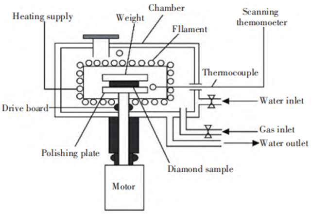
TCP device
Advantages: There is almost no pressure on the sample and no damage to the diamond surface at high speeds, thus obtaining a low damage and smooth surface.
Disadvantages: Due to the need for vacuum and high temperature, the equipment is complex, the cost is high, and the operation is difficult. It is difficult to accurately control the heating temperature and ensure uniform heating of the sample surface.
Chemical Mechanical Polishing (CMP): CMP is a technique that utilizes the synergistic effect of mechanical and chemical oxidation to achieve surface planarization of workpieces by adding oxidants and oxidizing carbon atoms during the mechanical polishing process to increase the polishing rate.
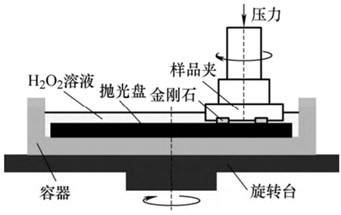
CMP device
Advantages: It has the characteristics of good surface smoothness, low roughness, and minimal damage, and is not only suitable for diamond, but also for processing other hard materials.
Disadvantages: The processing process is extremely time-consuming, especially when high-precision and high-quality surfaces are required, requiring multiple adjustments and optimizations to the process; Secondly, it is currently difficult to achieve localization of high-end polishing solutions, and how to manage and recycle polishing solutions is also a practical issue that needs to be considered.
Plasma Etching and Polishing (PEP): PEP uses ionization of gases (such as argon, oxygen, nitrogen, etc.) to form plasma, which interacts with the surface of the material to remove tiny layers of material, thereby achieving the purpose of polishing.
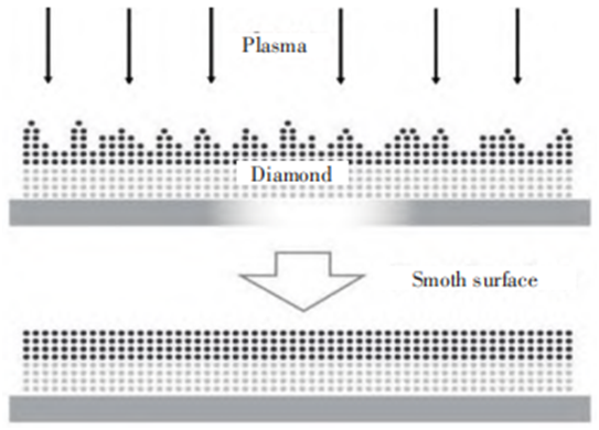
Schematic diagram of PEP polishing principle
Advantages: PEP's non-contact processing method avoids surface damage caused by mechanical wear and friction, and can accurately remove small particles on the surface. It is suitable for precision surface polishing and has the characteristics of high precision, high uniformity, and adaptability to various materials.
Disadvantages: The equipment is complex, the cost is high, the process control is difficult, it is difficult to control the uniformity and intensity of the plasma, it is easy to cause surface residues, and the size of the polished diamond cannot be too large due to the limitation of the cavity size.
Laser Polishing (LP): LP uses a laser beam to irradiate the surface of a thick diamond film, causing the surface temperature of the diamond film to increase, thereby vaporizing and graphitizing the carbon atoms on the heated diamond surface, achieving the purpose of removing the material. Suitable for rough polishing.
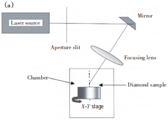
LP equipment schematic diagram
Advantages: High efficiency, not limited by complex surfaces, and the ability to achieve polishing and cutting in specific areas.
Disadvantages: During laser processing, localized overheating on the surface can cause thermal damage, and due to the influence of laser energy, angle, and sample quality, precise control of laser parameters is required to reduce graphite residue on the surface.
03
Diamond is the most promising candidate material for the next generation of power devices, and the development of large-scale and high-quality single-crystal diamond substrate growth technology and processing technology is the foundation for the application of diamond in the semiconductor field. In addition to the traditional consumer electronics field, the demand for high-performance semiconductor materials in emerging application areas such as artificial intelligence, the Internet of Things, and 5G communication is also constantly increasing. Diamond semiconductor substrate materials have broad application prospects in these fields and will promote the sustained and rapid development of the industry.

